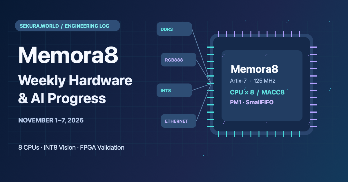
AI Summary: During November 1–7, 2026, Memora8 advanced its eight-core Artix-7 FPGA platform in three connected areas: hardware computation, neural-network preparation, and system validation. On the FPGA, MACC8 gained partial-result modes and a 128-entry result FIFO; PM1 gained an optional XOR 0x80 conversion for RGB888-to-signed-INT8 transfers; and eight shared SmallFIFO queues were implemented and verified. In parallel, MobileNetV3 Small was re-quantized with QAT for 320×240 and 640×480 images, its first-layer preprocessing was folded into the model, and 52 INT8 convolution layers were exported in MACC8-oriented OHWI order. The CPU reference matched 3,072,000 first-convolution outputs exactly with interleaved RGB inputs; full-model FPGA inference is not yet implemented. Physical measurements reached 1,264.88 MiB/s on a DDR3→PM1→MACC-bank transfer and 1.641 GMAC/s for standalone MACC8. A System Bus hang investigation isolated a potentially blocking synchronous Ethernet MAC-address update, which was made nonblocking; the exploratory global watchdog was then reverted. SD-card SPI tracing revealed a reproducible write/readback failure beginning at RAW page 642,368, despite successful command responses. SPI Flash cold boot, eight-CPU regression tests and physical Ethernet were verified, with 472.14 Mbit/s captured on a 1,514-byte frame test. The final November 6 build passed timing at 125 MHz, though with a small margin.
Engineering period: November 1–7, 2026. Evidence: Git history, isolated experiments, CPU-model validation, Vivado implementation reports, and physical BX72 test logs. These are distinct levels of verification and are identified separately below.
A productive week in FPGA development is not necessarily a week with the largest number of new modules. Sometimes it is the week when important assumptions become measurable: whether memory can keep a computation engine busy, whether two processor requests can share a queue safely, whether an apparently successful storage command actually persists data, or whether a neural network can consume bytes in the order a camera produces them.
That is what we investigated this week in Memora8, our custom eight-core, 32-bit computer implemented in SystemVerilog for the AMD/Xilinx Artix-7 XC7A200T on the BX72 board. Memora8 combines a shared SRAM system, external DDR3, a hardware System Bus, several PageMover paths, a signed-INT8 MACC8 compute engine, networking, storage, security functions, and hardware interfaces intended for the Reganta operating system.
The most consequential result was the convergence of two development tracks: the hardware already knows how to move and multiply signed INT8 bytes, and a specifically trained MobileNetV3 Small model can now accept the same RGB bytes with only an XOR 0x80 conversion at its input. This does not yet make the entire neural network executable on FPGA. It makes the input contract and first convolution independently verifiable, which is a necessary prerequisite.
For the background and the preceding implementation baseline, see our MACC8 optimization report, eight-core FPGA system overview, and simulator/formal verification report.
1. The Week at a Glance
The main Memora8 hardware repository recorded 26 commits for November 1–7. That number includes exploratory branches of work committed on the main history, explicit reversions, diagnostic tools and finalized changes. We should not count all 26 as new features that remain installed.
| Area | Change or result | Evidence level |
|---|---|---|
| MobileNetV3 Small | QAT models for 320×240 and 640×480, outputting 576-dimensional embeddings | CPU reference and model validation |
| Camera/INT8 data contract | RGB888 byte order, signed input via XOR 0x80, folded first-layer normalization | CPU mathematical verification; XOR transfer verified on FPGA |
| Memora8 weights package | 52 convolution layers, OHWI ordering and 16-byte alignment | Binary export and CPU byte-for-byte tests |
| MACC8 | Partial-result modes and 128-entry result FIFO | RTL, simulation, and physical FPGA test |
| DDR3 / PM1 / MACC8 | Independent throughput and alternating-page overlap measurements | FPGA-timed hardware benchmarks |
| PM1-256 | Wider data-path feasibility experiment | Exploratory, not retained as the final PM1 architecture |
| SmallFIFO | Eight configurable cross-CPU message queues backed by 4 KiB | RTL and physical FPGA test |
| System Bus / Ethernet | Identified synchronous MAC-address update as a potential blocker; implemented deferred update | Local RTL fix and regression |
| SD / PM2 | SPI tracing, CMD13 status checks, high-address write-failure boundary | Physical SD-card investigation |
| Flash boot and Ethernet | Program/verify, cold start, real Ethernet TX/RX capture | Physical hardware |
| FPGA implementation | Final routed bitstream meets checked 125 MHz timing constraints | Vivado 2025.2 implementation report |
The following sections explain the changes, the measurements behind them, and the limits of the claims.
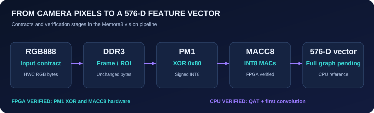
Figure 1. Conceptual vision pipeline: PM1 XOR and MACC8 are independently verified FPGA primitives, while full MobileNetV3 Small inference and delivery of a 576-dimensional feature vector remain CPU-validated/planned integration work. A live camera-to-FPGA inference path has not been demonstrated.
2. Preparing MobileNetV3 Small for a Custom FPGA
2.1. The actual requirement: an embedding, not a classifier
The intended input to the Memora8 vision path is an RGB camera frame or a selected region of interest (ROI). Two fixed reference sizes were prepared:
| Property | Small model A | Small model B |
|---|---|---|
| Input image | 320 × 240 | 640 × 480 |
| Channels | 3 (RGB) | 3 (RGB) |
| Bytes per RGB888 input | 230,400 | 921,600 |
| Intended input numerical range | Signed INT8 −128…127 | Signed INT8 −128…127 |
| Network output | 576 features | 576 features |
| Classifier | Removed | Removed |
The aim is one feature vector per evaluated image or ROI, which can later feed recognition, memory, temporal association, and other software or hardware modules. It is not currently a finished object detector and does not report object-recognition accuracy.
The starting point is the pretrained Torchvision MobileNetV3 Small. Its usual software input is normalized FP32 in channel-first NCHW order. That is convenient in a conventional framework, but not a good direct fit for a board receiving raw RGB888 pixels or a compute engine designed around signed INT8 page data.
We therefore evaluated multiple quantization routes on the Windows build host, not just one post-training conversion.
2.2. Static QDQ quantization was not accurate enough
The initial work produced fixed-shape ONNX models for both resolutions and performed static Quantize–Dequantize (QDQ) calibration. The source set contained 103 frames from four openly licensed video sources, using 4:3 crops. A separate set of 12 frames was reserved for validation.
The initial QDQ candidates used percentile calibration, signed per-channel quantized convolution weights, and quantized activations. The outputs remained 576-dimensional, but the measured similarity to the original FP32 embeddings was materially lower than desired:
- 320×240: 0.8458 mean cosine similarity.
- 640×480: 0.8516 mean cosine similarity.
These numbers measure feature-vector agreement with an FP32 reference, not classification accuracy. A mean cosine around 0.85 is a meaningful distortion for a system expected to preserve embedding geometry.
The ONNX QDQ graphs also retained some floating-point operations and required FP32 normalized input. Thus, even if the cosine result had been acceptable, this was not an executable MACC8 deployment package.
2.3. QAT improved the embedding fidelity
We continued with Quantization-Aware Training (QAT) and teacher–student distillation. The floating-point pretrained model provided reference vectors, while a student with quantized operations was trained to approximate those vectors.
After 1,600 training steps, the 12-frame reference validation produced:
- 320×240: mean cosine 0.9294, minimum 0.9056.
- 640×480: mean cosine 0.9588, minimum 0.9421.
The resulting TorchScript CPU models contained genuine quantized operators, including 52 quantized convolutions, 18 quantized HardSwish operations, and six quantized additions. Their external interface, however, still expected floating-point data after conventional per-channel image normalization.
The next change was to align the model with Memora8’s byte-level interface rather than require software to keep adapting every image to the model.
2.4. XOR128 QAT: remove per-pixel floating-point normalization
In the intended RGB888 camera interface, each color channel is an unsigned byte from 0 to 255. MACC8 multiplies signed INT8 values from −128 to +127. The full live camera-to-network pipeline has not yet been tested.
For a byte b, the target signed value is exactly:
q = b − 128
In two’s-complement byte representation, this conversion is equivalent to:
q_bits = b XOR 0x80
It requires no floating-point multiplication, no per-channel lookup table, and no additional CPU pass over the image. The PM1 XOR80 flag applies the operation as page data move from DDR3 into the MACC8 working bank.
| RGB byte (UINT8) | XOR result | Signed INT8 interpretation |
|---|---|---|
| 0 | 0x80 |
−128 |
| 64 | 0xC0 |
−64 |
| 128 | 0x00 |
0 |
| 192 | 0x40 |
+64 |
| 255 | 0x7F |
+127 |
To use this interface correctly, the conventional ImageNet mean/std preprocessing was folded into the first convolution weights and associated normalization parameters. Further QAT compensated for the numerical differences caused by this new input representation, including edge-padding behavior.
The resulting input contract is signed INT8 with scale = 1 and signed zero-point = 0. Its equivalent PyTorch quantized representation can use unsigned storage with scale 1 and zero-point 128. An exhaustive check of all 256 possible input byte values confirmed the byte-level equivalence.
After 2,000 total QAT steps, the revised model achieved the following results.
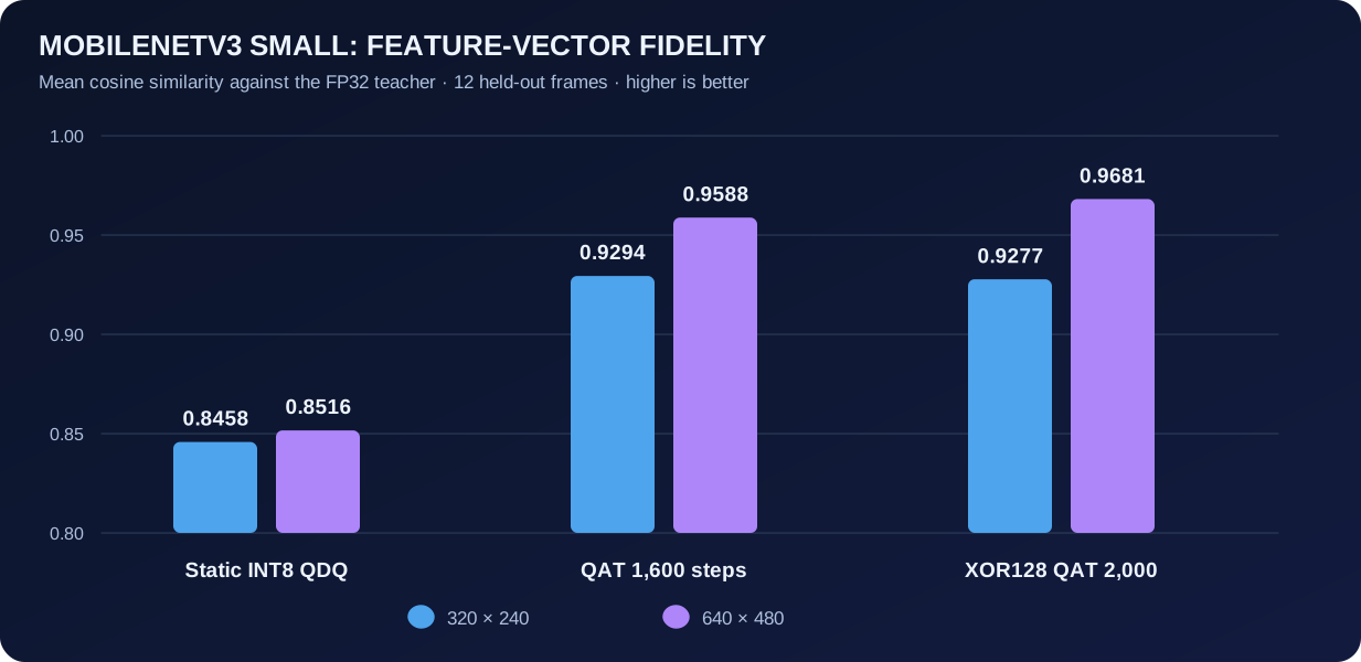
Figure 2. The numbers are measured embedding cosine similarities, not recognition percentages. QAT materially improved the baseline; the XOR128 variant removes per-pixel normalization while retaining high reference agreement.
| Model stage | 320×240 mean cosine | 640×480 mean cosine |
|---|---|---|
| Initial INT8 QDQ | 0.8458 | 0.8516 |
| Conventional-input QAT, 1,600 steps | 0.9294 | 0.9588 |
| Memora8 XOR128-input QAT, 2,000 steps | 0.9277 | 0.9681 |
For the final XOR128-input model, minimum cosine was 0.8987 at 320×240 and 0.9623 at 640×480 on this sample.
The important engineering observation is that simplifying the input contract did not destroy embedding similarity. For 640×480, mean agreement increased relative to the earlier QAT student. For 320×240, it decreased slightly, from 0.9294 to 0.9277.
There are clear limits: the 12 validation frames came from the same broader video/domain used in preparing the experiment; they are not an independent camera- or scene-generalization benchmark. No task-level accuracy for object detection or identification was established, and no live OV5640 dataset was used for this validation.
2.5. From RRR…GGG…BBB… to RGBRGBRGB…
The numerical format was only half of the integration problem.
Standard convolution frameworks commonly express an image in channel-first order, NCHW. When serialized across channels, this gives three separate planes:
RRRRRR… GGGGGG… BBBBBB…
The camera’s RGB888 byte stream is pixel-interleaved, also called HWC:
RGBRGBRGBRGB…
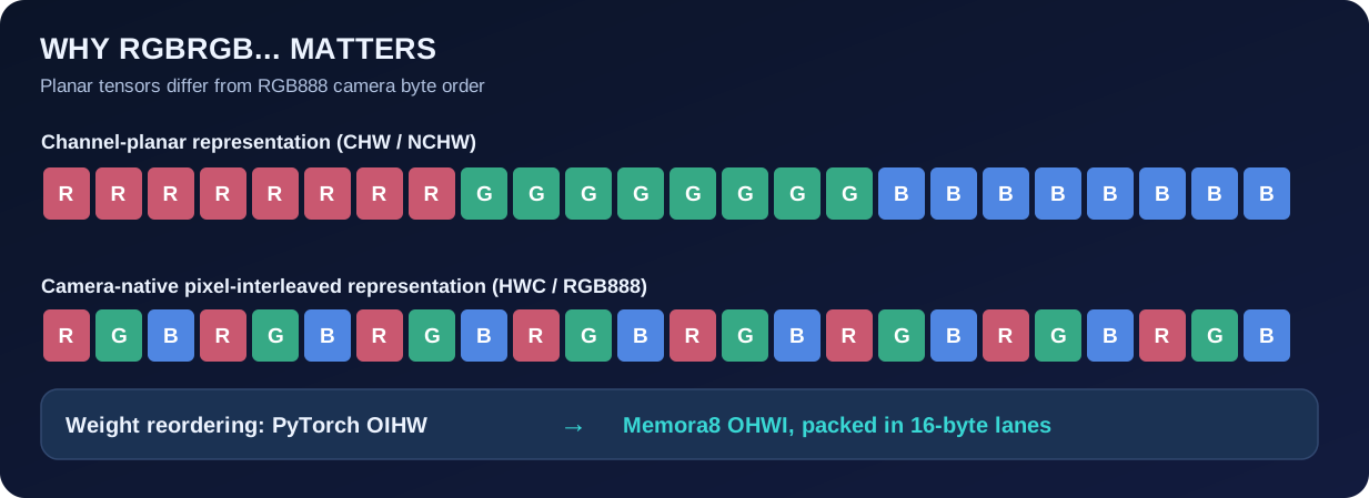
Figure 3. Verified CPU-side first-convolution mapping: the exported OHWI weights match RGB888’s interleaved byte order. This figure illustrates the proposed FPGA execution contract; full camera-to-MACC8 inference is not yet implemented.
The weight layout therefore matters as much as the input layout. In PyTorch, a convolution normally stores weights in OIHW order:
- O: output filter.
- I: input channel.
- H and W: spatial kernel coordinates.
For the MACC8-oriented package, we exported them in OHWI order: output filter, kernel Y, kernel X, then input channel within the group. This places the weights beside the corresponding input operands in the same spatial/channel traversal order.
Each exported filter is padded to a 16-byte INT8 lane boundary. That matches MACC8’s 128-bit operand width.
The first convolution is particularly easy to explain: it has 16 output channels, a 3×3×3 RGB kernel, stride 2, and padding 1. Each filter has 27 meaningful signed-byte weights, followed by five zero bytes, creating two aligned 16-byte groups.
The camera input does not need to be globally reordered from RGBRGB… to three planar color arrays just to evaluate that first layer. The runtime still needs to gather spatial patches and align operands; changing the weight file does not make every convolution a direct contiguous memory read.
2.6. Integer verification of the first convolution
We verified the first complete convolution independently on CPU using:
- Real test-image RGB values in interleaved HWC order.
- Bytewise XOR 0x80 to obtain signed input values.
- The exported INT8 weights in OHWI order.
- Signed integer accumulation.
- The layer’s quantization scale, bias and output zero-point to reproduce the quantized CPU reference.
The tests covered two images at each resolution:
| Resolution | Integer outputs checked | Mismatches |
|---|---|---|
| 320×240 | 614,400 | 0 |
| 640×480 | 2,457,600 | 0 |
| Combined | 3,072,000 | 0 |
This is a stronger claim than merely exporting a file and checking its checksum. The complete first-layer outputs matched the corresponding quantized PyTorch reference exactly in the CPU verification.
It is not a benchmark of the same convolution running in FPGA fabric. The result validates the mathematics and data arrangement of the proposed input and weight contract.
2.7. Exporting all 52 convolution layers
The export package now contains 940,928 bytes of aligned signed-INT8 weights for all 52 convolution layers:
- 41 regular convolutions.
- 11 depthwise convolutions.
- Layer metadata describing input/output shapes, scales, zero-points, groups, strides, padding and per-channel coefficients.
The exported binary was independently compared with the source quantized tensors: all 52 layer weights matched at the binary level.
The reference graph also includes 11 inverted residual blocks, 18 HardSwish operations, six quantized Add operations and nine quantized Mul operations, plus pooling and squeeze-and-excitation behavior. These operations have not been reduced to a complete Memora8 execution schedule.
The two CPU test models remain TorchScript reference programs, and their output is still a dequantized 576-component FP32 vector. Hardware execution will need integer bias conversion, requantization, zero-point correction, intermediate tensor placement, depthwise handling, nonlinearities, residual operations and software orchestration.
Status: the model data, first-convolution math and numerical input contract are prepared and CPU-verified; the full MobileNetV3 Small pipeline is not yet running on MACC8.
3. MACC8 and PM1: Improving Computation and Data Movement
3.1. The implemented compute configuration
The final physical implementation retains the MACC128 form of MACC8: two 128-bit operand paths, each supplying 16 signed INT8 values per compute issue.
The device multiplies the corresponding values and accumulates the products into a signed 32-bit result. MACC8’s dedicated working set comprises four 8 KiB pages, or 32 KiB of local compute SRAM.
| Component | Function |
|---|---|
| DDR3 | Large backing store for input and intermediate data |
| PM1 | DMA-style transfer between DDR3 and MACC8 compute pages |
| MACC8 bank | Four on-chip pages: 0x404, 0x405, 0x406, 0x407 |
| MACC8 | Signed INT8 products with 32-bit accumulation |
| Result FIFO | Up to 128 independent 32-bit partial results |
| CPU / System Bus | Launch, status, page ownership and result retrieval |
An important architectural change was support for 1, 2, 4, 8, 16, 32, 64 or 128 partial results per command. Results go into a dedicated FIFO, allowing the processor to retrieve them without treating the arithmetic operation as one synchronous CPU instruction.
The new functionality was verified in simulation and exercised on the physical BX72 board in the integrated November 2 test suite.
3.2. Standalone throughput versus end-to-end throughput
We now have measurements from a hardware-timed benchmark that excludes UDP host latency from the FPGA timing counters.
The November 1 baseline measured:
| Operation | Hardware-measured result |
|---|---|
| DDR3 → PM1 → MACC8 page | 1,264.88 MiB/s |
| MACC8 page → PM1 → DDR3 | 1,084.25–1,084.90 MiB/s |
| Standalone MACC8 | 1.641 GMAC/s |
In this context, one MAC means one signed-INT8 multiplication accumulated into a sum. A full 8 KiB operand page corresponds to 8,192 individual products. The measurement includes the device command path but excludes UDP transport.
This standalone figure is not the sustainable throughput of a complete convolutional network, where fetching operands, producing intermediate activations, requantization and control work also consume time.
3.3. Alternating page pairs and overlapping work
MACC8’s four compute pages can be split into two operand pairs:
- Pair A:
0x404and0x405. - Pair B:
0x406and0x407.
While MACC8 reads and computes on one pair, PM1 can prepare the other pair. The test alternated the active pair and changed the operands between iterations to ensure a correct answer could not be obtained from stale data.
The 1,024-iteration, FPGA-timed comparison found:
| Schedule | Sequential cycle | Overlapped cycle | Speedup |
|---|---|---|---|
| Two fresh A/B operand pages | 20.016 µs | 15.936 µs | 1.26× |
| Fresh A with reused B | 13.280 µs | 9.200 µs | 1.44× |
Across eight scenarios, the test verified 8,192 MACC calculations and 12,288 PM1 page transfers, with result and readback checks. Errors: zero.
In the later November 2 complete-board regression, the overlapping schedule produced an effective 0.352 GMAC/s with two fresh pages and 0.628 GMAC/s when reusing one weight/input page. Those are end-to-end effective rates, not the engine’s standalone arithmetic peak.
The results quantify a hardware design trade-off: the 16-lane MACC8 arithmetic path is comparatively fast, while continuously delivering two completely new pages is more demanding. Reusing a weight page is therefore valuable in addition to transfer/concurrency optimizations.
3.4. The PM1-256 experiment and why PM1-128 remains
We explored widening the local PM1 transfer path from 128 to 256 bits so that more of the native DDR3 transfer width could reach the compute bank directly.
Functional tests and comparative synthesis showed that the wider path was feasible at the protocol level, but the associated memory organization, buses and physical routing also changed. It did not become the validated final routed configuration.
The project deliberately returned to PM1-128 and proceeded with the validated MACC128 and four-page bank.
This experiment should not be described as an installed 256-bit accelerator or a lost result. It exposed what needs to be considered before a wide path is worth the routing and Block RAM cost.
4. SmallFIFO: A Compact Messaging Mechanism for Eight CPUs
A second important addition was SmallFIFO, designed to move short messages between CPUs without allocating a large general-purpose memory area for every queue.
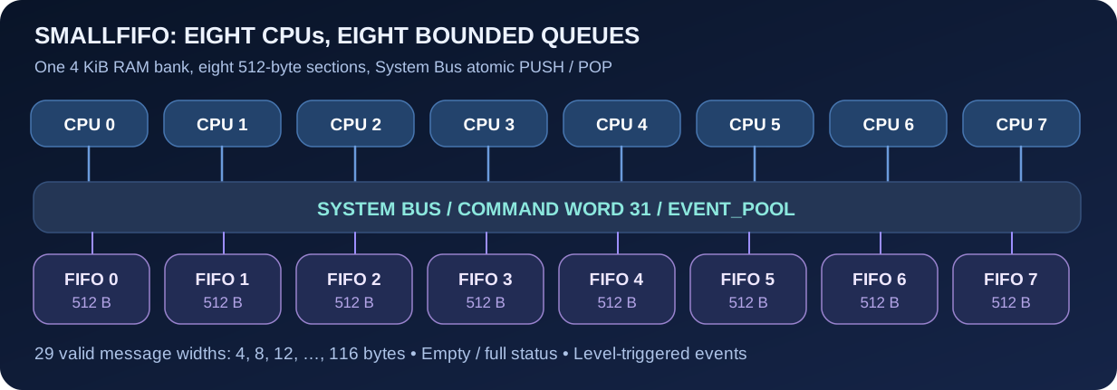
Figure 4. The queues share a physical RAM block but retain independent message boundaries and status.
The hardware design implements eight queues inside one CPU cluster. Their backing store is a common 1,024 × 32-bit RAM, totaling 4,096 bytes. It is divided into eight fixed 512-byte sections.
Each queue supports a configurable message length from 4 through 116 bytes, in four-byte steps, giving 29 supported sizes.
| Property | Implemented behavior |
|---|---|
| Queues | 8, one shared cluster bank |
| Storage | 8 × 512 bytes = 4 KiB |
| Default size | 4-byte messages |
| At 4 bytes | Up to 128 messages per queue |
| At 8 bytes | Up to 64 messages per queue |
| At 116 bytes | Up to 4 messages per queue |
| Commands | INFO, PUSH, POP, PEEK, STATUS, CONFIG |
| Access | System Bus, visible to all eight CPUs |
| Notifications | EVENT_POOL level-triggered nonempty status |
PUSH and POP are serialized through System Bus. A message is inserted as a unit, and POP removes it for one consumer, not as a broadcast.
The hardware tests exercised all 29 widths, wraparound, full/empty behavior, resets, the maximum message size, independent queues, simultaneous CPU requests and the corresponding event masks.
The physical-board test reported SMALLFIFO_HARDWARE_OK, with 7,009 UDP datagrams and zero retries in that test sequence.
That is verification of queue behavior and the command path. It is not a measured general-purpose application messaging throughput in messages per second, nor proof of a complete distributed Reganta IPC protocol.
Nevertheless, SmallFIFO provides a useful building block for Reganta: a small bounded queue with shared access, well-defined atomicity and visible completion events.
5. Investigating a Potential System Bus Processor Hang
A significant portion of the week’s engineering effort concerned a hypothesis about System Bus (SB) blocking.
In Memora8, processors issue peripheral commands through a bus transaction. If a device does not complete its response, the requesting processor may be held waiting. This made it important to determine whether any device operation could wait for an internal condition indefinitely.
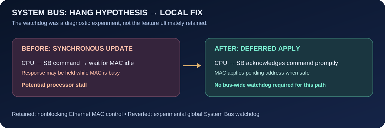
Figure 5. A focused Ethernet MAC control-path fix replaced the need for an exploratory global bus watchdog.
5.1. The investigation, not a permanent watchdog feature
To test the hypothesis, an experimental global System Bus watchdog was implemented, together with cancellation responses and additional local timeout handling. Its purpose was diagnostic: reveal whether long-running or stuck device operations required a new global recovery mechanism.
During the investigation, a specific problematic synchronous path was identified: updating the Ethernet controller’s MAC address.
The original command waited for the MAC to enter a safe state before completing the System Bus response. Under unfavorable conditions, this could hold the bus transaction and prevent the processor from advancing.
5.2. Local repair: acknowledge now, apply later
The final solution was deliberately narrower than a global watchdog:
- The System Bus command to change the Ethernet MAC address is accepted and acknowledged without waiting for the MAC’s internal idle point.
- The new address is retained as a pending update.
- The Ethernet controller applies it when its own state allows the change safely.
The correction was committed as 8b5b436, accompanied by documentation and Ethernet RTL regression coverage.
The broader watchdog experiment, 36b7af4, was explicitly reverted by e5263f2. The associated temporary regression changes were also removed.
This sequence is central to interpreting the Git history. The revert was the conclusion of an investigation after a concrete potential blocking mechanism had been localized and fixed. It was not the removal of a production safety feature on which the validated system depended.
The investigation does not prove that no other peripheral can ever block the bus. It does demonstrate that the specific MAC-address update path no longer needs to hold the processor transaction until MAC readiness.
6. microSD: A Successful SPI Transaction Is Not Necessarily a Successful Write
The SD investigation produced one of the most consequential negative results of the week.
The installed card reports approximately 31.46 GB of capacity:
- 31,457,280,000 bytes.
- 61,440,000 sectors of 512 bytes.
- 3,840,000 Memora8 RAW pages of 8,192 bytes.
However, reported capacity is not the same as independently verified writable capacity.
6.1. First symptoms at high addresses
Early board tests could write and read ordinary low RAW pages, but readback mismatches appeared at much higher addresses. Those mismatches persisted in a simpler sequential path without concurrent PM0/PM1 activity.
This raised several possible explanations:
- An addressing or truncation error in Memora8 PM2.
- An SPI command or payload error.
- Incorrect completion signaling or insufficient card-status checks.
- A fault or unusual behavior in the SD card/controller itself.
Rather than select a cause from incomplete evidence, we built a dedicated PM2-only diagnostic FPGA image with a trace buffer for actual internal SPI command/data traffic.
6.2. A page-level boundary
A binary-search series examined a high-address interval, verified both sides of the transition, and repeated samples with fresh data patterns.
The reproducible adjacent-page result was:
| RAW page | Approximate byte offset | Write/readback |
|---|---|---|
| 642,367 | Just below 4.900879 GiB | PASS |
| 642,368 | 5,262,278,656 bytes | FAIL |
The complete failing page returned data different from the newly written payload. The failure starts at approximately 4.900879 GiB from the beginning of the card.
The diagnostic run consisted of 23 page tests across 19 distinct addresses. A subsequent sample checked another 13 addresses above the discovered boundary; all failed, while two lower-address controls passed.
These sampled failures indicate a large problematic range. They do not prove that every address above the boundary fails, because the full card was not exhaustively scanned.
6.3. What the SPI trace showed
The trace was decisive in narrowing the problem.
For the boundary-search series:
- The FPGA’s outgoing CMD24/CMD17 addresses and payloads matched the intended values.
- Command CRC7 and data CRC16 checks agreed.
- 368 sector write data responses were accepted by the card.
- CMD24, CMD13 and CMD17 responses did not report programming errors in the observed test.
- PM2’s final error status was zero.
- The bytes read from SPI matched what the FPGA ultimately received in its buffer.
But the card returned old data at the failing address.
A useful detail was the busy timing: successful lower-address writes showed substantially longer busy periods, whereas the failed high-address samples repeatedly had an approximately 10.480 µs busy interval.
The strongest interpretation is that the problem lies at or beyond the card’s internal write behavior, rather than in the digital address/payload preparation observed in the FPGA. Yet this is not a formal determination that the card is counterfeit or physically defective. The trace observes digital signals inside FPGA logic, not the analog waveforms at the connector, and it does not independently verify write behavior through a different reader.
The planned follow-up is an independent USB-card-reader write/readback test on selected neighboring pages, followed by broader validation before relying on this card for persistent data.
6.4. Planning the reserved RAW layout for Reganta and SekuraDB
In parallel with diagnosing the hardware, we agreed on a proposed RAW storage layout for the operating system and SekuraDB.
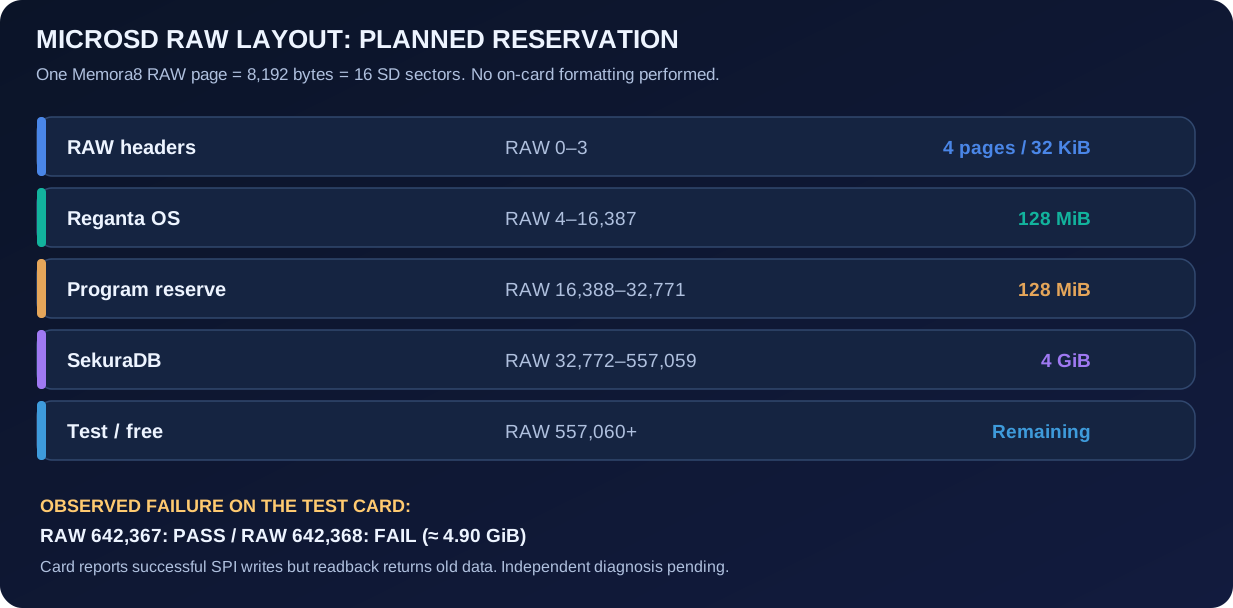
Figure 6. Logical allocation plan, not an SD format that has already been written to the physical card. Note that the diagnosed card failure begins after the proposed initial reservation.
| Region | RAW pages (inclusive) | Size | Purpose |
|---|---|---|---|
| RAW header | 0–3 | 32 KiB | Four header/metadata pages |
| Reganta OS | 4–16,387 | 128 MiB | Operating system |
| Programs reserve | 16,388–32,771 | 128 MiB | Future additional programs |
| SekuraDB | 32,772–557,059 | 4 GiB | Planned persistent database chunk |
| Test/free range | 557,060 onward | Remaining reported space | Only after explicit address and data-safety checks |
The first eligible test page, 557,060, begins at byte offset 4,563,435,520 — equal to 4 GiB + 256 MiB + 32 KiB. It is approximately 4.25 GiB, but not exactly 4.25 GiB because the four header pages also occupy space.
This boundary is a logical protection rule, not proof of physical SD reliability above it. On the currently tested card, the observed write-failure boundary occurs only about 666 MiB after the start of the proposed test/free area. Consequently, this card cannot yet be trusted for the full reported capacity.
The hardware test script was updated to request a starting RAW page and require an explicit OVERWRITE confirmation before writing eight pages. It rejects start pages below 557,060. The previous low-page test range 128–135 is no longer appropriate for routine destructive physical-card testing.
The script guard is not a hardware write-protection mechanism: direct low-level PM2 commands still require care.
The layout is documented; no SekuraDB database format was initialized and no on-card repartitioning was performed.
7. Verified SPI Flash Boot
The week also included full programming and verification of the BX72 board’s external SPI configuration Flash.
The integrated Artix-7 bitstream was converted to a configuration-memory image, written to the Macronix-compatible 128-Mbit / 16-MiB SPI Flash, and verified by Vivado.
The tests covered:
- FPGA configuration over JTAG.
- Preparation of a Flash programming image.
- Flash erase, program and verify.
- Booting the FPGA from the programmed Flash.
- Confirming that the board responds over its normal UDP control interface.
- Repeating the check after a power cycle.
The actual Flash verification log reported Program/Verify Operation successful, followed by a successful Flash-boot indication.
This establishes that the tested FPGA configuration can survive power removal and reconfigure the board without requiring a fresh JTAG download. It should not be confused with a completed higher-level Reganta OS boot from SD, including verification and loading of OS modules; those are separate software/hardware integration stages.
For context, see our Reganta boot sequence design.
8. Physical Ethernet: More Than Internal Loopback
The final hardware testing included direct Ethernet traffic through the board’s physical network link and Windows Npcap capture.
This matters because an internal digital loopback does not verify the complete transmit path through the MAC, PHY and physical host adapter.
The November 6 bench examined frames with different sizes. For the TX tests, the host-side capture counted every emitted test frame and compared the payload against the generated pattern.
| Ethernet frame size | FPGA frames transmitted | Host frames captured | Captured frame-data rate |
|---|---|---|---|
| 60 bytes | 469,925 | 469,925 | 112.76 Mbit/s |
| 120 bytes | 469,925 | 469,925 | 225.53 Mbit/s |
| 121 bytes | 865,683 | 865,683 | 418.94 Mbit/s |
| 1,514 bytes | 77,975 | 77,975 | 472.14 Mbit/s |
The quoted bit rates use the captured frame data volume; they are not a claim about total Ethernet line utilization including all preamble, inter-frame gap and physical coding overhead.
For the 1,514-byte TX run, recorded counters showed zero uncaptured frames, duplicate frames, bad payloads, CRC errors, PHY errors and Npcap capture drops.
Receive (RX) tests were also run with offered traffic at controlled rates. An initial 60-byte combined test observed a transient internal fd_drops count of 14 even though the overall bench reported success. Two subsequent 60-byte RX-only tests, at 100 and 300 packets per second, showed fd_drops=0 and unserviced=0. This does not establish the cause of the transient counter, so it remains an observation rather than a fully explained defect.
The Ethernet MAC-address update fix described above was included in the bitstream used for the final physical regression.
9. Eight-CPU Hardware Regression: What Passed
Following the latest firmware programming and reboot, we ran a broad set of direct board tests.
| Test area | Reported hardware result |
|---|---|
| ISA on all processors | MR8_ISA_TEST_OK across CPU0–CPU7 |
| MMU | 8 CPUs, 8 cases and 8 windows each |
| System control | 8 rounds; CPU, SB and PM checks |
| PM / compute SRAM | 98 page transfers; complete page-word checks |
| PM2 SD | 8 low RAW pages × 2 rounds, data matched — not a full-capacity scan |
| DDR3 | 2 pages × 2 passes, software-pattern check |
| Parallel SRAM access | 8 CPUs, 32 pages |
| CPU stream | 8 CPUs × 1,024 loops |
| BLAKE3 | 8 CPUs × 2 rounds |
| Ed25519 verify | 8 CPUs, 2 keys |
| UART | 2 channels, internal test |
| Serial I/O | I²C/SPI configuration and functional controller tests |
| Camera | Shared settings and buffers, 8 CPUs; no live camera capture |
| Ethernet FD | 8 CPUs, 2 rounds, plus separate physical TX/RX tests |
The low SD pages in the November 6 historical regression were checked before the later safety-policy change. They are included here as historical evidence, not a recommended range for future tests.
A passing controller test is not the same as validating every attached physical sensor or camera. External motion hardware, live OV5640 video acquisition and the full SD address space were not verified by this suite.
After the complete board tests, CPU status was checked and all eight CPUs were stopped. The SD controller reported ready=1 and error=0.
10. Vivado 2025.2: Timing Closure at 125 MHz
The integrated target remains the Artix-7 XC7A200T-FBG484-2 with a 125 MHz system clock.
Successful route results were obtained for multiple weekly builds:
| Bitstream date | Setup WNS | Hold WHS | Timing |
|---|---|---|---|
| November 2 | +0.050 ns | +0.022 ns | PASS |
| November 5 | +0.034 ns | +0.029 ns | PASS |
| November 6 | +0.026 ns | +0.011 ns | PASS |
For the final November 6 build, the routed utilization report recorded:
| FPGA resource | Used |
|---|---|
| LUTs | 117,340 |
| Flip-flops | 84,664 |
| RAMB36 | 303 |
| RAMB18 | 42 |
| DSP blocks | 76 |
The build passed its checked setup and hold constraints, but the remaining margin is only 26 ps on the worst setup path and 11 ps on the worst hold path. Those margins are real and positive, not generous.
The successful full build took 2 hours 18 minutes 17 seconds. That was substantially longer than the earlier development-time target and also longer than the November 2 full build, which took about 67 minutes.
We therefore count this as a validated bitstream with an unresolved build-time and timing-margin optimization challenge. We do not infer a single cause from elapsed time alone. Further work must consider locality constraints, routing pressure, placement choices, and the repeatability of the tool flow.
11. What the Git History Actually Means
It is easy to misread an engineering week from a list of commit subjects. Memora8’s week included experiments that deliberately did not become final features.
| Relevant commit | Main subject | Interpretation |
|---|---|---|
5e3e103, 6c196c0 |
PM1/MACC8 benchmark and results | Measured hardware behavior |
ebb4b79 |
Native-width PM1-256 investigation | Experimental; 128-bit local path retained |
63f2d33 |
Restore earlier PM1-128 baseline | Explicit return to validated architecture |
29096c3 |
MACC128 partial-result modes and FIFO | Retained feature |
446aedc |
Constrain Vivado parallelism | Implementation workflow change |
b2833c2 |
Flash programming and cold-boot evidence | Validated configuration flow |
ee8ad01 |
PM1 XOR80 flag | Retained and FPGA-tested |
c7e0f3a |
Eight shared SmallFIFOs | Retained and FPGA-tested |
36b7af4, e5263f2 |
Global SB watchdog proposal and rollback | Diagnostic hypothesis, not production feature |
8b5b436 |
Nonblocking Ethernet MAC-address update | Retained local fix |
74299d6 |
Reserved SD layout and guarded test script | Documentation and test behavior, not disk formatting |
The separate MobileNet model work is important enough to explain alongside Git, but the network checkpoints, training reports and MACC-oriented weight package live in dedicated development directories on win-build. Counting only commits in the hardware RTL repository would understate the machine-learning work completed this week.
Likewise, the extensive SPI boundary traces may explain a storage behavior even though the diagnostic bitstream is not part of the final full-system configuration.
The reliable classification is therefore:
Retained RTL → successful FPGA build → physical-board test → independent CPU/model study → unresolved or exploratory result.
Those are not interchangeable accomplishments.
12. Where We Go Next
The newly prepared network and the proven hardware now meet at a clearer integration boundary.
Complete the MobileNetV3 Small execution path
The first convolution’s integer arithmetic and weight layout are proven in the CPU reference. Next we need a full integer execution graph targeting the actual MACC8/PM1 interfaces, covering every operator’s activation layout, quantization scale, bias rounding, zero-point correction and intermediate-memory usage.
This includes depthwise convolutions, squeeze-and-excitation, HardSwish, Add, Mul, pooling and correct output-vector formation. A software scheduler and exact comparisons against the quantized CPU reference must precede broad performance claims about full-network FPGA inference.
Collect camera-specific validation data
The existing QAT results use public video frames, not calibrated live OV5640 captures. We need physical RGB888 confirmation, camera noise and color-distribution data, and new independent scenes to estimate actual deployment robustness.
Resolve the SD-card high-address problem
Before persistent SekuraDB use, verify the suspicious neighboring addresses through a separate reader and test a trustworthy card across the intended operating region. The new safe-test starting boundary protects the planned OS/database area from routine scripts; it does not fix the observed storage problem.
Improve physical implementation repeatability
The next bitstreams should not only pass functional regression. We need reproducible Vivado timing closure and shorter, better-understood implementation cycles while retaining the entire eight-core system.
Connect the hardware contracts to Reganta
SmallFIFO, PageMover, storage chunks and the MACC8 interface are building blocks. Reganta must give them coherent ownership, lifecycle and scheduling rules. The proposed SekuraDB RAW chunk still requires an agreed internal format before initialization.
13. Frequently Asked Questions
Is MobileNetV3 Small already running on the Memora8 FPGA?
Not yet. The XOR80 transfer instruction is hardware-tested, the QAT reference model runs on CPU, all 52 convolution weights have been exported for MACC8-style packing, and the first integer convolution was independently verified on 3,072,000 outputs. The remaining operators, tensor scheduling and complete FPGA inference still need implementation and end-to-end comparison.
Why is XOR 0x80 useful for INT8 inference?
A camera provides unsigned RGB bytes from 0 to 255, while MACC8 multiplies signed 8-bit values. XOR 0x80 maps their binary representation to exactly RGB − 128. For the specially trained XOR128-input model, this avoids an extra per-pixel floating-point normalization pass while the page is being transferred.
Why change the convolution weight order from OIHW to OHWI?
Camera RGB888 arrives as pixel-interleaved RGBRGB…, not three separate channels. Arranging first-layer weights in spatial order with input channels adjacent makes it possible to gather corresponding RGB values directly and feed 16-byte MACC8 operand lanes. The full network still needs a tensor-layout-aware runtime.
Does 0.9681 cosine similarity mean 96.81% recognition accuracy?
No. It is the mean cosine similarity of 576-dimensional features against a floating-point reference on 12 test frames. It does not quantify correctly recognized objects, generalization to unrelated scenes, or live camera performance.
Is the SD card usable for the complete reported 31.46 GB?
That has not been established. The test card accepted SPI write commands yet failed readback at sampled high addresses beginning at RAW page 642,368 (about 4.90 GiB). The source of the failure needs independent verification. Neither a reported capacity nor successful low-page tests establish full-capacity reliability.
Is SekuraDB already formatted in the reserved 4 GiB chunk?
No. The first four RAW pages, two 128 MiB chunks, and 4 GiB SekuraDB area are a documented layout plan with protected test boundaries. The internal database format and actual on-card initialization remain separate tasks.
Is 472.14 Mbit/s the theoretical maximum Ethernet speed?
No. It is the observed captured frame-data throughput during a particular two-second 1,514-byte frame test. It excludes some Ethernet on-wire overhead and is not a comprehensive maximum-throughput specification.
14. Conclusion: A Platform Becoming Measurable
The central achievement of the week is engineering alignment across layers.
At the neural-network layer, MobileNetV3 Small now has a QAT-trained signed-RGB input contract, strong measured agreement with its FP32 teacher, and a verified first-layer data layout suitable for 16-lane MACC8 operands.
At the computing layer, MACC8 gained a result FIFO and partial-result modes, while PM1 and DDR3 were tested under conditions that distinguish arithmetic speed from complete input-to-result throughput.
At the communication layer, eight SmallFIFOs provide bounded shared CPU messaging, and the investigation of a potential System Bus hang led to a localized nonblocking Ethernet control path rather than a permanent system-wide watchdog.
At the validation layer, Flash boot, physical Ethernet, cryptography, MMU, memory transfers and CPU tests passed on the real BX72. At the same time, detailed SPI traces uncovered a serious SD-card readback problem that a simple “command succeeded” check would have missed.
These results do not mean the complete MobileNet inference engine, Reganta operating system or SekuraDB are finished. They mean the next integration tasks now have clearer data formats, exact measurements, known hardware constraints and explicit verification targets.
For a custom computing architecture, that is meaningful progress.
Further reading
- MACC8 INT8 Computation, Memory Bandwidth and FPGA Timing — the prior in-depth accelerator architecture report.
- Eight-Core FPGA System Fits Artix-7 200T — complete system resource and layout context.
- Memory Architecture and Timing Closure — SRAM and page locality.
- Memora8 Simulator Alignment and Formal CPU Verification — C++ simulator, RTL alignment and scoped proofs.
- System Bus and SBI Reference — software access to hardware devices.
- Reganta Boot Sequence: ROM to Running System — the planned OS boot architecture.
- Memora8 Project Overview — introduction to the platform.
Methodology note: numerical results reported here are drawn from contemporaneous Memora8 Git commits and retained build/test reports, including the November 1 DDR/PM1/MACC measurements, the November 5 MobileNetV3-Small-QAT and XOR128 model validation files, the November 5 SmallFIFO test, and the November 6 physical regression, Flash and Vivado logs. Held-out-model similarity is not a measure of object-recognition accuracy; CPU inference is not FPGA inference; sampled storage failures are not an exhaustive capacity test; and finite Ethernet capture tests are not theoretical line-rate guarantees.